


Epoxy Adhesive

TEL:18925129293


Semiconductor Packaging Adhesive Stirring & Defoaming Solution
date:2026-09-03author:小施Working Condition Requirements
• Material Type: Semiconductor packaging adhesives (Die Attach, Molding Compound, Underfill, Dam Fill, Encapsulant, etc.)
• Initial State: Semiconductor packaging adhesives are high‑precision electronic‑grade materials with extremely strict bubble‑control requirements. Nano‑scale micro‑bubbles exist inside the colloid. Even tiny residual bubbles can cause chip packaging failure and impair product yield and reliability.
• Processing Target: Thoroughly remove nano‑scale micro‑bubbles from semiconductor packaging adhesives to achieve uniform, fine texture with zero residual bubbles. Meet high‑precision semiconductor packaging process requirements for die attach, molding, underfill and dam‑and‑fill, and guarantee long‑term chip reliability.
Comparison Before and After Improvement
Before Improvement — Pain Points of Traditional Processes
Semiconductor packaging adhesives are widely used in integrated circuits, chip packaging, memory chips, sensors and other semiconductor fields. Their quality directly determines chip performance and long‑term reliability. Nevertheless, semiconductor packaging imposes stringent bubble‑control standards, and conventional processing methods face multiple challenges:
• Difficult removal of nano‑scale bubbles: Semiconductor packaging adhesives feature high viscosity and high precision requirements. Conventional vacuum degassing chambers cannot effectively eliminate nano‑scale micro‑bubbles, and residual bubbles lead to voids and cracks in packaging layers.
• Voids in die attach: Residual bubbles in Die Attach adhesives result in incomplete bonding between chip and substrate, forming concentrated thermal resistance zones. Local overheating occurs during chip operation, which severely degrades performance and service life.
• Molding compound defects: Bubbles inside Molding Compound trigger bubbles, cracks and delamination of packages. Water vapor intrusion accelerates chip corrosion and greatly reduces product yield.
• Uneven underfill: Bubbles in Underfill adhesives cause non‑uniform filling and uneven stress distribution between chip and substrate, which easily leads to cracking failure under thermal cycling.
• Low product yield: Incomplete bubble removal by traditional methods brings high packaging defect rates, low yield and sharply increased costs.
Solution
• Nano‑scale vacuum defoaming + planetary motion: Under vacuum conditions, powerful shearing and convection generated by rotation‑revolution planetary motion gradually float and extract nano‑scale micro‑bubbles from semiconductor packaging adhesives. Nano‑level defoaming effect is achieved to satisfy rigorous bubble‑control requirements of the semiconductor industry.
• Void‑free die attach: Fully defoamed Die Attach adhesives produce void‑free cured layers with complete chip‑to‑substrate bonding, evenly distributed thermal resistance and stable chip operating temperature.
• Dense and defect‑free molding compound: Defoamed Molding Compound cures into compact structures free of bubbles, cracks and delamination. Water vapor ingress is blocked, and long‑term chip reliability is greatly improved.
• Complete and uniform underfill: Bubbles are completely eliminated from Underfill adhesives for full and even filling. Stress distribution between chip and substrate becomes uniform with outstanding thermal‑cycling reliability.
Advantages of Stirring & Defoaming Machine
• Nano‑level defoaming: Vacuum environment combined with planetary motion efficiently removes nano‑scale micro‑bubbles from semiconductor packaging adhesives and meets strict bubble‑control standards for semiconductor manufacturing.
• Uniform and fine colloid: Gentle and even rotation‑revolution planetary motion delivers consistent, fine adhesive texture without residual bubbles for superior packaging quality.
• Precisely controllable parameters: Rotation speed, duration and vacuum degree are adjustable. Process parameters can be precisely optimized for different packaging adhesives to secure optimal defoaming performance.
• High efficiency & time‑saving: The whole stirring‑defoaming procedure finishes within minutes, replacing long‑time static degassing and greatly boosting production efficiency.
• Non‑contact & pollution‑free: Non‑contact design avoids physical contact with materials and secondary contamination, preserving electronic‑grade purity of semiconductor packaging adhesives.
• Compatible with high‑precision packaging: Treated packaging adhesives fulfill process requirements for high‑precision semiconductor packaging including die attach, molding, underfill and dam‑and‑fill.
Test Conditions
Item | Parameter |
Model | SIE‑MIX90 |
Test Material | Semiconductor packaging adhesives (Die Attach / Molding Compound / Underfill, etc.) |
Test Rotation Speed | 1800 rpm |
Test Time | 4 min |
Vacuum Degree | ‑95KPa |
Effect Comparison Before and After Stirring
Comparison Dimension | Before Stirring | After Stirring |
Bubble Content | Contains nano‑scale micro‑bubbles, voids appear after packaging | Nano‑scale bubbles completely removed, compact void‑free packaging |
Die Attach Quality | Incomplete bonding, concentrated thermal resistance, local overheating | Complete bonding, uniform thermal resistance, stable chip temperature |
Molding Compound Quality | Risk of bubbles, cracks and delamination in packages | Compact defect‑free packages, no cracks or delamination |
Underfill Performance | Uneven filling and irregular stress distribution | Complete and uniform filling with even stress distribution |
Product Yield | High packaging defect rate and low yield | Excellent packaging quality with significantly improved yield |
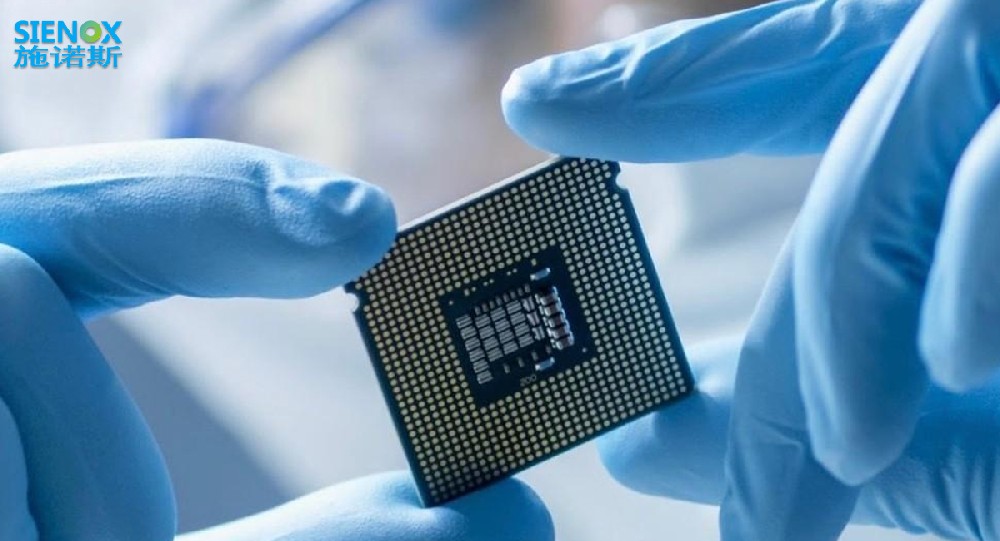
Mature Application Fields
✅ Integrated Circuit Packaging
✅ Die Attach
✅ Molding
✅ Underfill
✅ Dam & Fill
✅ Memory Chip Packaging
Related recommendations
Adhesive Materials

SIENOX Planetary Mixer-Defoamer Empowers High-Reliability Bonding Solutions for Structural Adhesives
Stirring‑Defoaming Solution for Glue Materials in Consumer‑Electronics Industry
Semiconductor Packaging Adhesive Stirring & Defoaming Solution
Perhaps you still need....
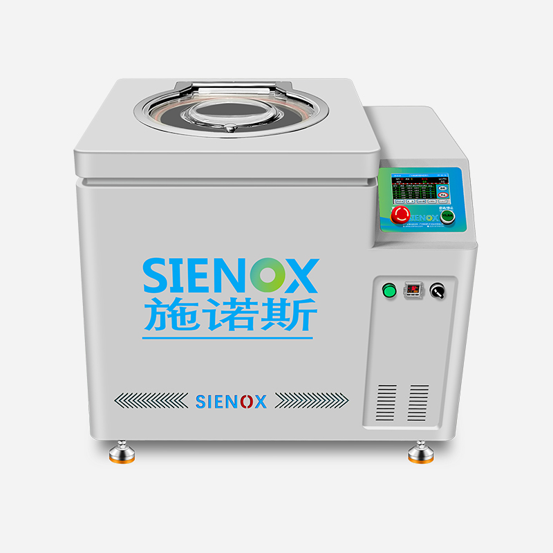
行星式真空脱泡搅拌机 SIE-MIX1000plus
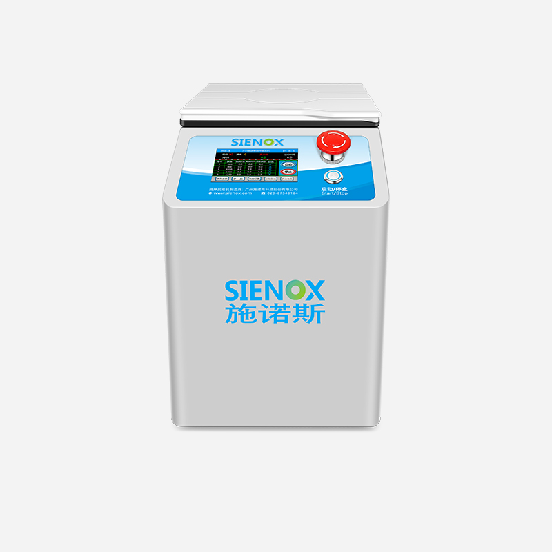
实验室行星式搅拌脱泡机 SIE-SV200
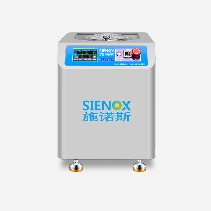
SIENOX行星式脱泡搅拌机 SIE-CV300
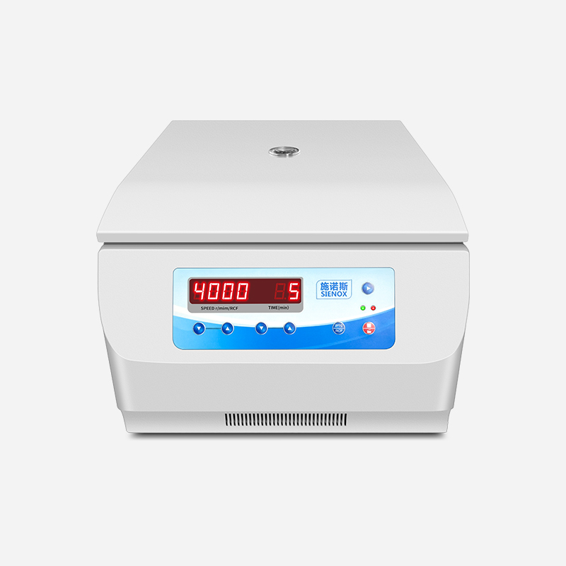
离心脱泡机 SIE-C006
About SIENOX
广州施诺斯(SIENOX),20年脱泡机设备研发与生产的源头厂家
超过1800种材料脱泡案例
纳米级脱泡,满足不同材料多段搅拌除泡需要,支持定制
资质齐全,荣获多项国家专利,联系我们可免费试样