


Epoxy Adhesive

TEL:18925129293


SIENOX Planetary Mixing‑Defoaming Machine: High‑Precision Preparation Solution for Semiconductor Packaging Materials
date:2026-09-02author:小施In semiconductor packaging, wafer‑level bonding and advanced manufacturing processes, homogeneity, low‑stress performance and ultra‑high cleanliness of packaging materials are core guarantees for chip reliability and yield. SIENOX planetary mixing‑defoaming machine adopts non‑contact revolution‑rotation mixing technology and nanoscale vacuum deaeration system. It delivers zero‑contamination and high‑consistency process assurance for high‑sensitive materials such as Epoxy Molding Compound (EMC), Die‑Attach Film (DAF) and photoresist, helping semiconductor manufacturing break through the bottleneck of micron‑level defect control.
Challenges | SIENOX Solutions | Value Improvement |
Thermal stress caused by nano‑filler agglomeration | Revolution‑rotation centrifugal force field (0‑2000 rpm adjustable), realizes uniform dispersion of silica / diamond fillers (CV value<3%), thermal conductivity fluctuation ≤±5% | Chip heat dissipation efficiency increased by 40%, packaging warpage reduced to 0.1 mm/m |
Delamination failure induced by micro‑bubbles | Multi‑stage gradient vacuum deaeration, simultaneous mixing and deaeration, bubble size controlled<5 μm, residual content<50 ppm | Interfacial bonding strength reaches 150 MPa, packaging yield>99.9% |
Risk of metallic ion contamination | Non‑contact design, materials only contact ceramic / PTFE containers, certified cleanliness under quality management system, metallic impurities<0.1 ppb | Meet purity requirements for advanced processes below 28 nm |
High‑precision temperature control requirement | Temperature control system inhibits resin pre‑curing, process window extended to 8 hours | Curing shrinkage<0.02%, wafer‑dicing chipping rate reduced by 80% |
Semiconductor Scenario‑Based Application Cases
Flip‑Chip Underfill Adhesive
SIENOX equipment realizes loss‑free dispersion of nano‑silica slurry with filler distribution uniformity up to 99.2%. Combined with vacuum deaeration, colloid fluidity increases by 30% and filling time is shortened to 3 seconds. Applied in 5G millimeter‑wave chip packaging with void rate<0.001%.
Wafer‑Level Packaging (WLP) Photoresist
For thick‑film photoresist (SU‑8 series), SIENOX customized low‑shear mixing mode eliminates micro‑bubbles under vacuum. Film‑thickness uniformity (3 μm@100 μm) reaches ±1.5%. Adopted in TSV through‑silicon‑via process, via yield rises to 99.5%.
High‑Thermal‑Conductivity Thermal Interface Material (TIM)
With SIENOX planetary mixing technology, composite slurry of boron nitride / silver nanowires achieves thermal conductivity over 25 W/m·K and resistivity<1×10⁻⁵ Ω·cm. Used for GPU chip heat dissipation, junction temperature drops by 18 ℃ and performance stability improves by 45%.
Core Advantages of SIENOX Semiconductor Solutions
Sub‑micron‑level defect control: Intelligent control system monitors material status in real‑time and automatically corrects mixing parameters;
Ultra‑clean process chain: Fully‑closed inert‑gas protection module with oxygen content<10 ppm, suitable for BGA solder paste preparation
Full‑process controllability: Supports MES system docking to realize digital closed‑loop of formula management‑production‑quality inspection.
Related recommendations
Adhesive Materials

SIENOX Planetary Mixer-Defoamer Empowers High-Reliability Bonding Solutions for Structural Adhesives
Stirring‑Defoaming Solution for Glue Materials in Consumer‑Electronics Industry
Semiconductor Packaging Adhesive Stirring & Defoaming Solution
Perhaps you still need....
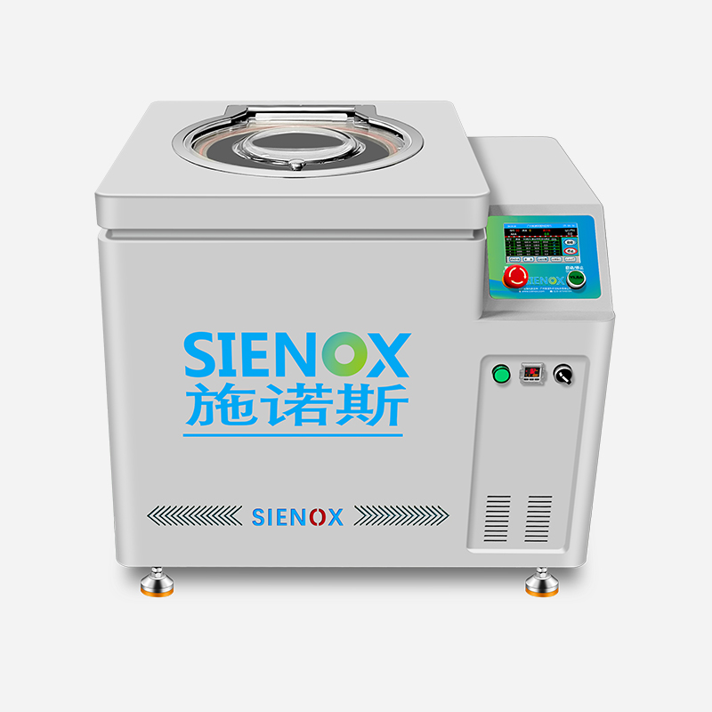
行星式真空脱泡搅拌机 SIE-MIX1000plus
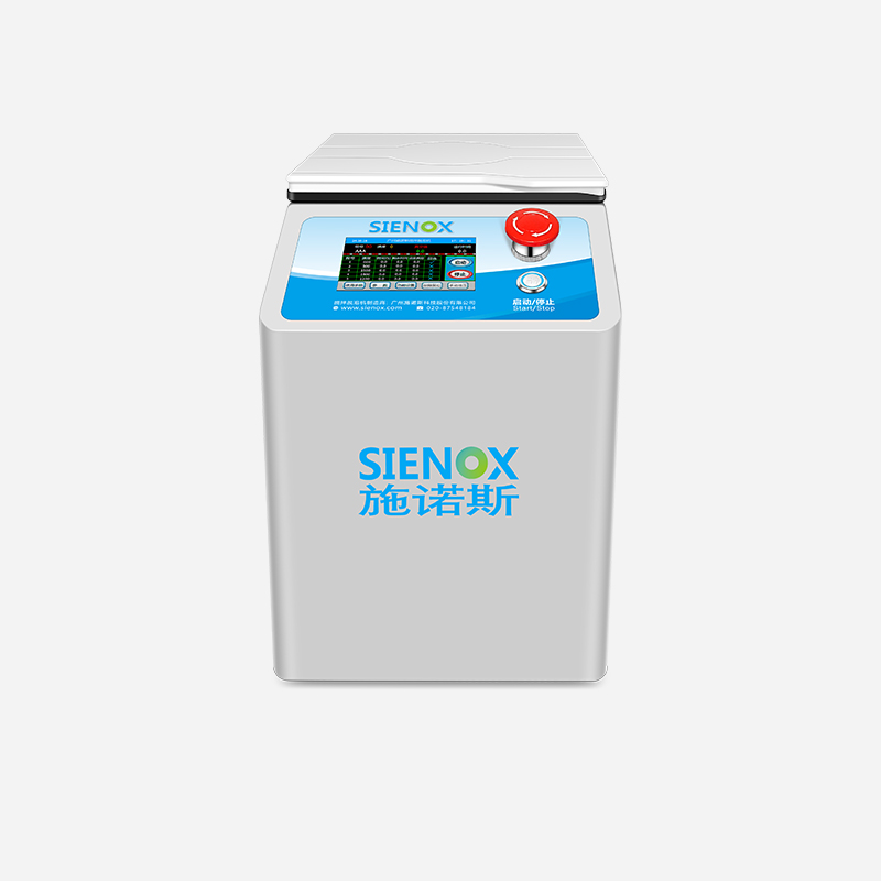
实验室行星式搅拌脱泡机 SIE-SV200
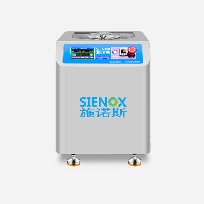
SIENOX行星式脱泡搅拌机 SIE-CV300
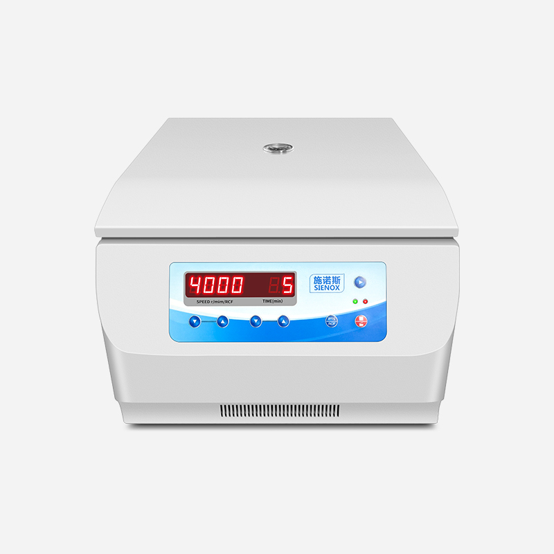
离心脱泡机 SIE-C006
About SIENOX
广州施诺斯(SIENOX),20年脱泡机设备研发与生产的源头厂家
超过1800种材料脱泡案例
纳米级脱泡,满足不同材料多段搅拌除泡需要,支持定制
资质齐全,荣获多项国家专利,联系我们可免费试样